We started DarkVision with a simple vision: build the world’s most advanced ultrasound imaging systems. What we didn’t initially realize was that to develop systems that were orders of magnitude better than what was available, we’d have to become experts and pioneers at every part of the technology stack. What initially started as a simple vision grew into an enormous set of challenges across all the engineering disciplines, whether it be mechanical, materials, electrical, software, firmware, data-science, AI/ML, or machine vision.
We’ve now built 3 generations of core ultrasound imaging technology and at each stage, we’ve pushed the engineering limits of what’s possible. This means taking on all the core design challenges to ensure the technology stack is perfectly synchronized so there are no bottlenecks that throttle performance. From the custom-built sensor arrays (up to 24,576 transducers) to the visualization software that processes multi-petabyte datasets, we are setting a new standard in what ultrasound systems are capable of.
Building from the Ground Up
Developing expertise at every level of the technology stack didn’t come easily or immediately. We broke the problems we were trying to solve down to their fundamentals. We recruited experts from a diverse set of industries, including aerospace and medical imaging, to take a fresh look at what we wanted to build. From there we removed red tape and gave our engineers the decision rights to enable faster, higher quality innovation at every layer.
Capturing Data: Sensors that Rewrite the Rules
Data quality starts at the tip of the spear: the sensor head (this is where our ultrasound transducers—which send and receive ultrasound signals—are located).
Conventional ultrasound technology uses single, oversized elements, sometimes more than an inch across, that simply can’t capture the fine resolution needed for asset owners need to fully understand discrete failure mechanisms (like cracks in composite materials, pinhole corrosion in steel, or delaminations in carbon fiber). We wanted more: higher resolution, greater reliability, imaging mode freedom, and a smaller footprint to fit anywhere that needs inspection.
The answer was dense, solid-state arrays—first spanning in one dimension and later in two dimensions, depending on the product. This meant fitting hundreds or thousands (up to 24,576, to be exact) of individual elements into what would have usually only fit single digit numbers on conventional tools. This sort of sensor density cannot just be bought off the shelf. It required custom machines like dicing saws most commonly found in silicon foundries, that can do repeatable cuts with positioning accuracy down to 0.0004 inches.
But just having more sensors doesn’t mean that you’re going to have superior data. It’s how you use all these sensors to send and receive wavefronts. More on that in the next section.
These high-density arrays have no moving parts which means they are much more robust. And we need every ounce of robustness when pushing our technology 20,000 feet underground (experiencing up to 20,000psi and 302 degrees Fahrenheit) or cruising through a pipeline at 600 feet per minute.
In the end, designing and fabricating solid-state transducer arrays required years of design, prototyping, testing, and validation (check out our Prototyping blog, coming soon). But the result? Higher resolution and data fidelity than anything available on the market.
Electronics & Firmware: Taming Data Tsunamis
To power DarkVision’s high-density ultrasound arrays, both literally and figuratively, our engineers design and build custom printed circuit boards (PCBs) that capture, sort, compress, and store petabytes of data in an efficient and organized manner. Given that our front-end data rates are over 1.5 terabits per second, off-the-shelf electronic designs simply wouldn’t cut it. This drives the need for high-density boards, and in some cases, custom-designed silicon chips, to handle the massive data flow.
Our PCBs often exceed 20 layers, with tracings intricate enough to challenge even the most seasoned engineers in telecommunications or medical equipment manufacturing. We incorporate core technologies, chipsets, and components that would typically be found in smartphones and high-end gaming systems into our products. Doing so was unheard of in the industrial inspection space; starting from first principles (and not getting sucked into the “we must do what was done before” mentality) was the first step in building a game changing technology.
And as we mentioned before, these electronics enable DarkVision to deploy advanced imaging modes, where each transducer element precisely sends and receives sound waves to create constructive interference patterns and pinpoint focus. In turn, that allows us to capture and store far greater detail—detail that is required to detect surface scratches as shallow as 0.01 inches, adapt dynamically to the unique geometry of inspected assets, and capture all defect types in a single pass over the target material.
Managing such colossal data volumes (petabytes uncompressed) demands proprietary lossless compression algorithms, developed by our electrical and software engineers, to fit all information within the onboard storage. Without these compression algorithms, the data pipeline would stagnate, or we would have to truncate useful signal information right at the initial data capture stage—something that we’re adamantly against.
And just to top it off, these electronics must fit into compact packages (e.g. that can be deployed inside pipes as small as 2 inches in diameter) compressing what once would have filled half a room 20 years ago into assemblies that would fit into the palm of your hand.
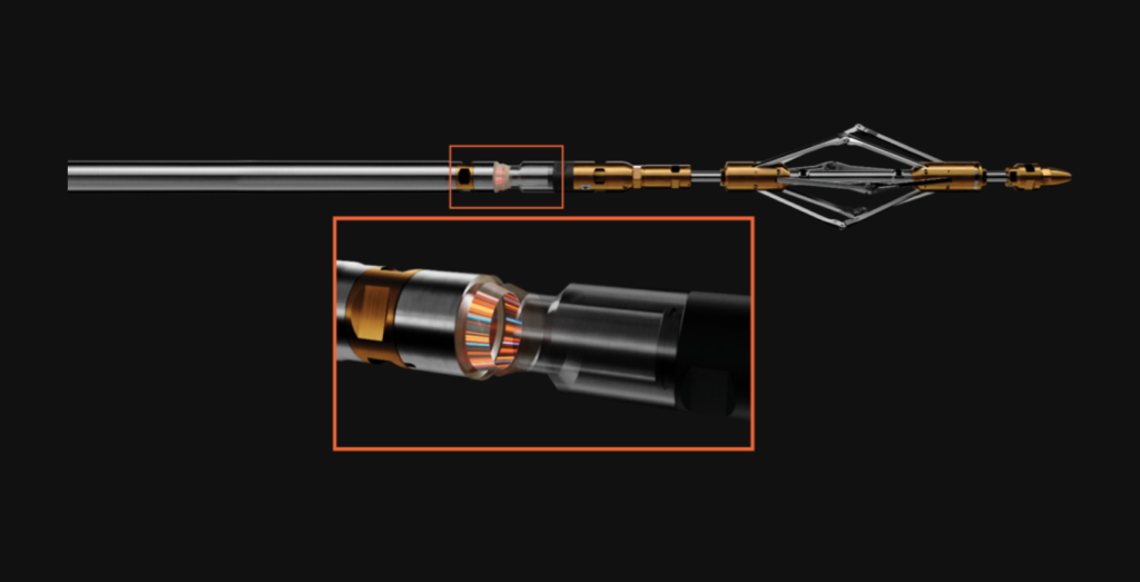
Mechanical Packaging: Surviving the Impossible
Our technology is deployed in some of the harshest environments on the planet. We engineer our mechanical housings (that contain highly sensitive electronics) to endure extreme temperatures and pressures, harsh manufacturing conditions, and the physical abuse often experienced in industrial environments.
For example, our first-gen product, HADES, inspects some of the planet’s deepest and hottest wells (think 15,000 feet below ground at 300°F, in harsh, opaque, corrosive fluids). KRAKEN, our pipeline inspection platform that was launched in 2025, finds cracks and corrosion at resolutions of 0.01in while flying through a pipeline at nearly 600ft/minute. Neither of these environments are exactly clean or friendly.
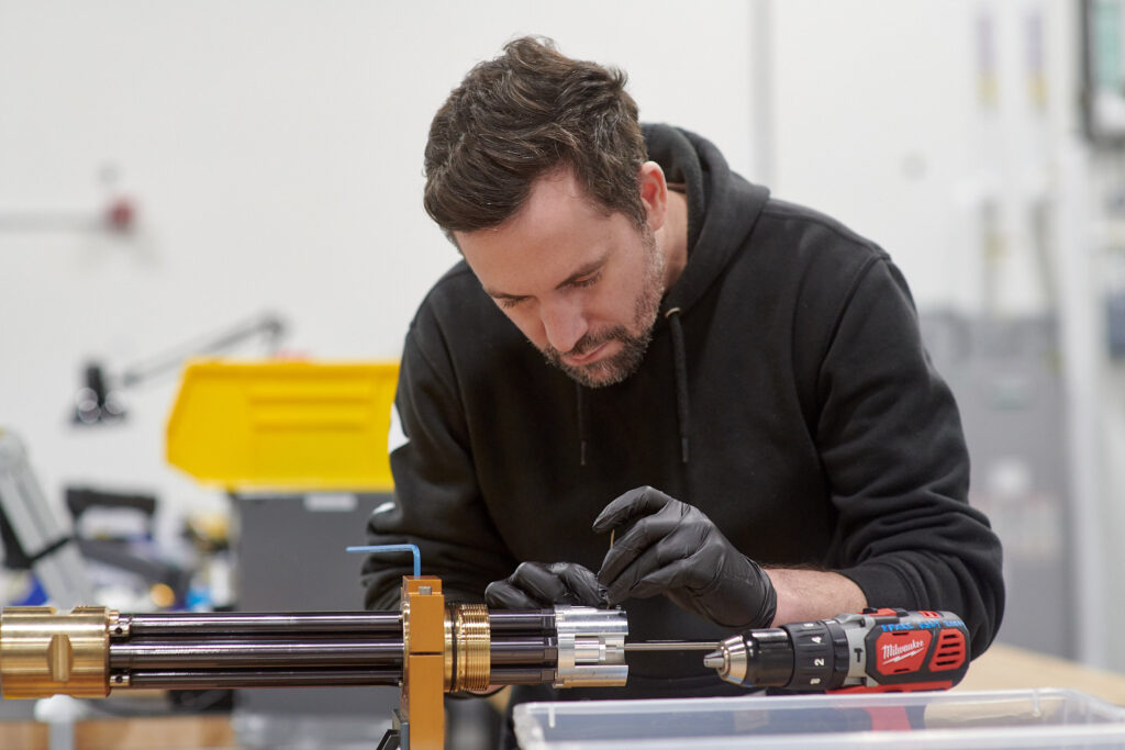
Our engineers have the challenge of protecting our sensitive arrays and electronics in rugged packages capable of resisting corrosive fluids, extreme heat and pressure, intense shock loads, and rough handling. To achieve this, we leverage advanced materials like Inconel and Hastelloy, develop custom epoxies that resist cracking under immense loads, and rigorously simulate and test designs to failure (sometimes spectacularly). This ingenuity extends to inventing specialized CNC, wire bonding, and soldering programs to work with these tough materials, as well as custom jigs and robotics to handle submillimetric connections—a testament to the demanding and precise craftsmanship required.
AI Data Processing: Finding Needles in Haystacks
Processing petabytes of ultrasound data is a monumental challenge, but making sense of it is where the real value lies. Our system is designed to uncover the “needles in the haystack” (as in find minuscule and potentially catastrophic defects in large amounts of base material) like finding hundreds of thousands of corrosion pinholes in a 100,000-tonne military ship hull, subtle wall thickness variations in thousands of miles of pipe coming off a production line, or 0.01-inch cracks in a pipeline spanning hundreds of miles.
With billions of ultrasound images captured during inspections, manually identifying these defects would be impossible. That’s why we’ve built our own custom AI models from the ground up that been training on our large high-fidelity datasets for years. We now have 17 different models that are commercially being used with several more in development, training and testing. Once the data is uploaded to our AWS-supported processing network, we spin up thousands of GPUs to run dozens of these AI models in parallel to parse the information, highlighting defects and areas of concern. This automation-assisted analysis ensures asset owners can act quickly to maintain safety and integrity.
But it doesn’t stop there. Just finding something that’s problematic doesn’t give the engineers all the information they need to identify the root cause and fix it. They need to understand the context and circumstances that led to that failure mechanism arising. And that’s where our visualization platform comes in.
Data Visualization: Clarity in Complexity
More data is only valuable if it can be easily digested and translated into actionable insights. This is true whether that means patching a breach in a well, replacing an aircraft component before failure, swapping out a pipeline section with low rupture pressure, or optimizing gas well pressure to store more fuel for a harsh winter.
To make this data digestible and easy to understand, we developed visualization software from scratch that present our enormous datasets in intuitive 2D and 3D formats.
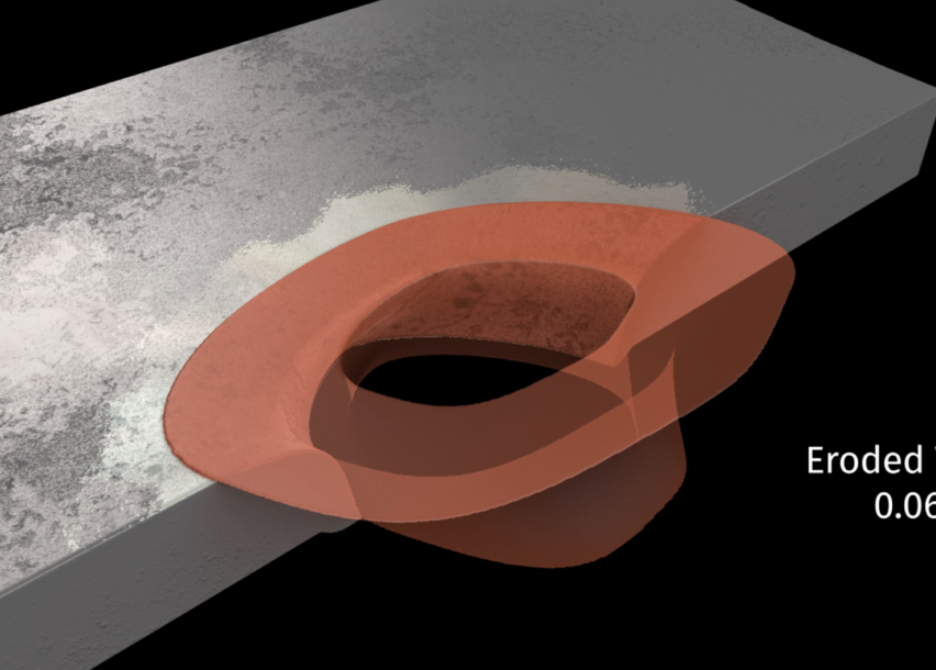
This capability is only possible because of the exceptionally high resolution of our data. Trying to diagnose these micro-defects with standard data is like trying to perform deep-ultraviolet lithography using a flashlight. When your ‘pixel size’ is larger than the feature you are trying to measure, the data smears into a blurred diffraction pattern. High-resolution data moves us past the ‘diffraction limit’ of standard sensors, turning a blurry blob of heat into a distinct geometric failure point. Without precise data, analysis tools, and a way to display the data in an easy-to-understand way, engineers will often be forced to make educated guesses at what the root cause was. This can lead to false positives (causing operators to spend money to fix a problem that wasn’t real), or worse, can lead to false negatives (downplaying the significance or a problem or missing it entirely). We believe that visualizing data in three dimensions through high-resolution renderings is how people can understand the full context of whatever problem is plaguing their asset.
What’s Next: The 3rd Generation Tech Stack
The next leap in our technology is even more ambitious. It demands that we push the physical limits of our hardware further than ever before. We are diving deep into the realm of extremely dense 2D arrays, proprietary silicon chips, and a machine learning structure that translates petabytes of ultrasound data into easy-to-understand results from units that would fit in the palm of your hand. This shift will make the industry fundamentally rethink how high-fidelity data is acquired and processed. Ultrasound imaging still has vast untapped potential and DarkVision is leading the technological innovation of the future.


Newsletter Signup
By clicking Submit you’re confirming that you agree and consent to our Terms and Conditions.